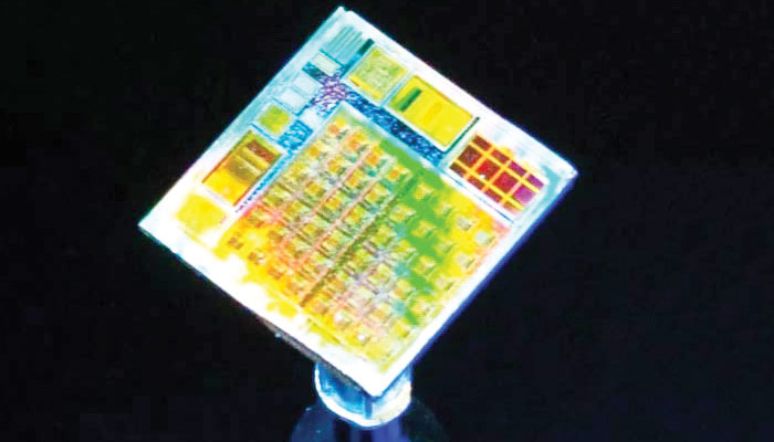
Dr. Mario Lanza of King Abdulaziz University of Science and Technology in Saudi Arabia and his colleagues have created the world’s first two-dimensional microchip. This chip performs high quality work at low power. Experts say that designing and manufacturing this thin chip were both big challenges. It was only because of the discovery of graphene, the thinnest layer of graphite in 2004, that this chip was made possible.
Making it viable was also a challenge. But now experts have made it possible. According to Mario Lanza, the traditional silicon-based “complementary metal oxide semiconductor” (CMOS) circuit was first used as a basis. He then prepared a six-dimensional (hexagonal) toady material from boron nitrate that was etched onto a very thin copper foil, then carefully placed on a CMOS circuit, electrodes were formed and the circuit was fabricated by photolithography. Thus cells were formed which consisted of a transistor and a memristor.
The thickness of the two-dimensional boron nitrate layer was only 18 atoms or 6 nanometers. A current was passed through them which was controlled, then the Toddy chip was tested for a long period of time and it showed excellent performance.
setTimeout(function(){
!function(f,b,e,v,n,t,s)
{if(f.fbq)return;n=f.fbq=function(){n.callMethod?
n.callMethod.apply(n,arguments):n.queue.push(arguments)};
if(!f._fbq)f._fbq=n;n.push=n;n.loaded=!0;n.version=’2.0′;
n.queue=[];t=b.createElement(e);t.async=!0;
t.src=v;s=b.getElementsByTagName(e)[0];
s.parentNode.insertBefore(t,s)}(window,document,’script’,
‘https://connect.facebook.net/en_US/fbevents.js’);
fbq(‘init’, ‘836181349842357’);
fbq(‘track’, ‘PageView’);
}, 6000);
/*setTimeout(function(){
(function (d, s, id) {
var js, fjs = d.getElementsByTagName(s)[0];
if (d.getElementById(id)) return;
js = d.createElement(s);
js.id = id;
js.src = “//connect.facebook.net/en_US/sdk.js#xfbml=1&version=v2.11&appId=580305968816694”;
fjs.parentNode.insertBefore(js, fjs);
}(document, ‘script’, ‘facebook-jssdk’));
}, 4000);*/


